Well, I think I arrived at a decent solution to the planar embedding:
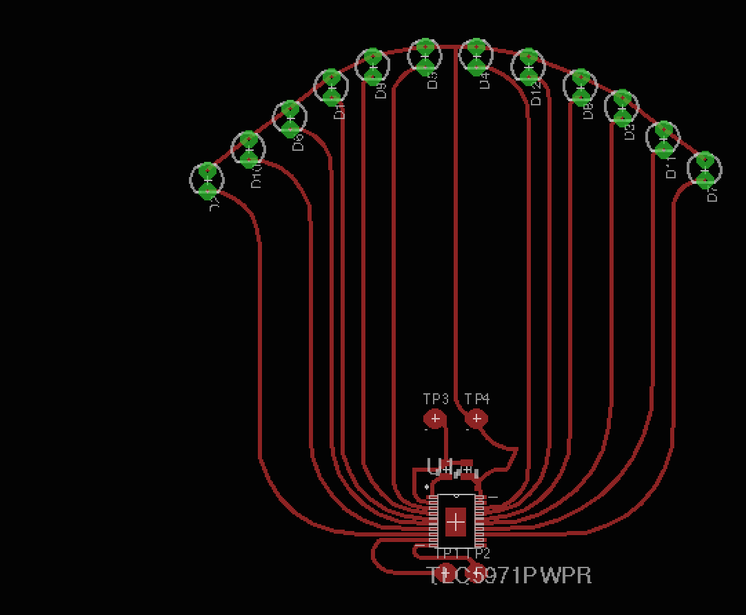
The issue is really those two pads in the middle. They provide a power and ground signal for the circuit. This graph is totally flat, and needs no jumpers, but I have to connect to those pads from a physical location near the other two pads below the IC. Previous iterations just had jumpers connecting two points on the board – now, wires just run from those pads through grooves in the brim to the rest of the hat. Done and done. I was going to have to connect wires to the board anyways to send the data to the LED driver.
This image represents fairly faithfully what will be etched in copper. It does need a bit of cleanup though. Turns out the hard part of this process is finding a decent quality laser printer that I don’t have to pay to use. Also ferric chloride is hard to find, but many hobbyists are now using a slightly more aggressive mix of hydrogen peroxide and muriatic acid, which are available at most hardware stores.
A lot of the past few weeks have been figuring out how to get this PCB trace routing software to work. For practice, I ended up making a few boards that break out the functionality of the music visualization chips I’ve been using. Once I get them cleaned up I’ll see if there’s a way to upload the files here.
Also been practicing with soldering SMD components. These things are tiny – capacitors and resistors are smaller than half a grain of rice. The soldering technique involves hot air and a solder paste instead of iron and wire. There’s just not enough room to maneuver the tip of an iron around these things.
This week will be sourcing fabric and finishing the assembly of the brim. The rest of the electronics are taken care of, modulo tweaks to code to catch bugs and so forth. This brim has taken a bit of time to get done, but I think it’ll come together nicely.