5/15/2015 Final Semester Update

To sum up my work this semester, Professor Ponto has asked me to answer some questions about my project.

js

1) Describe your final project. What have you accomplished over the course of the semester?

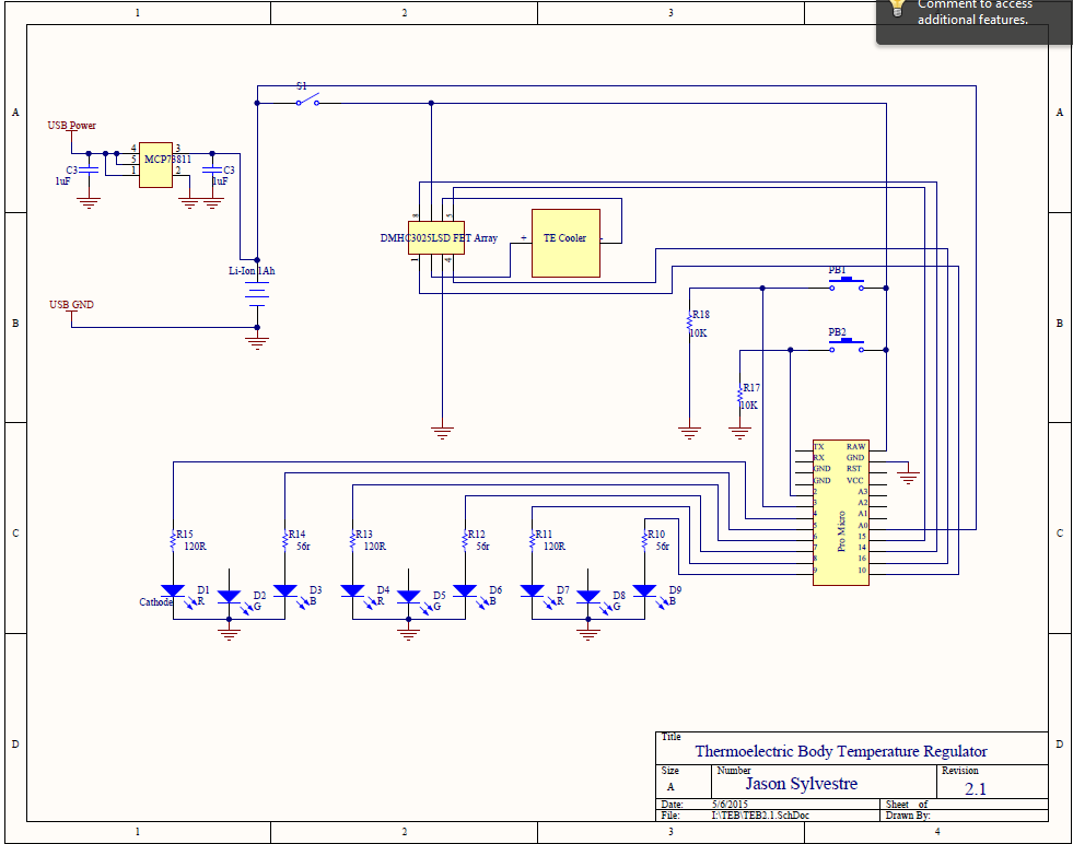
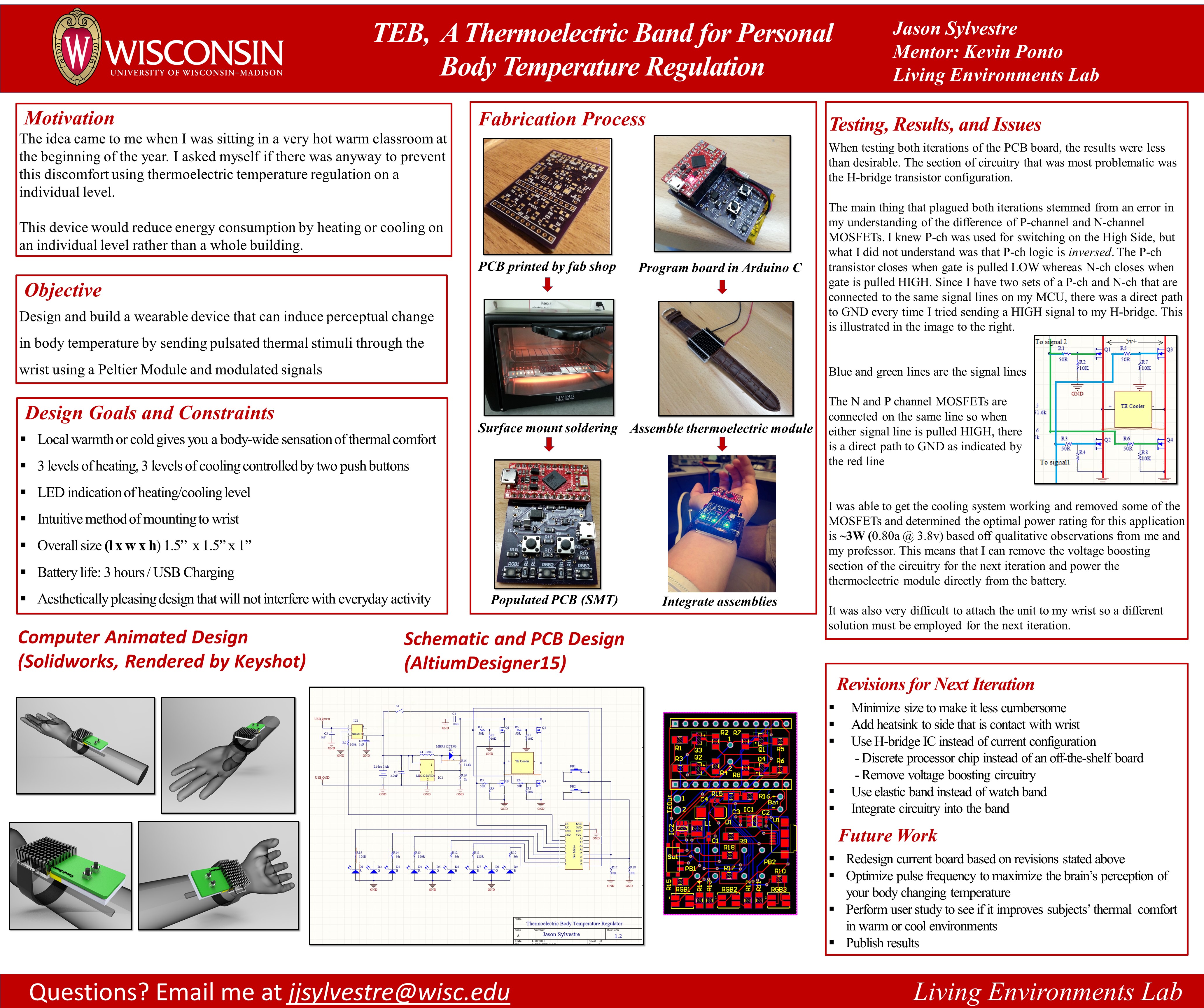
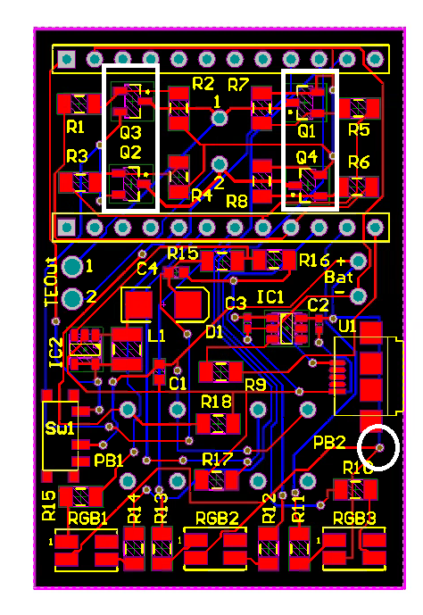
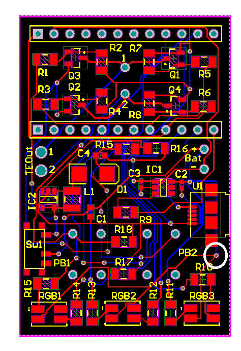
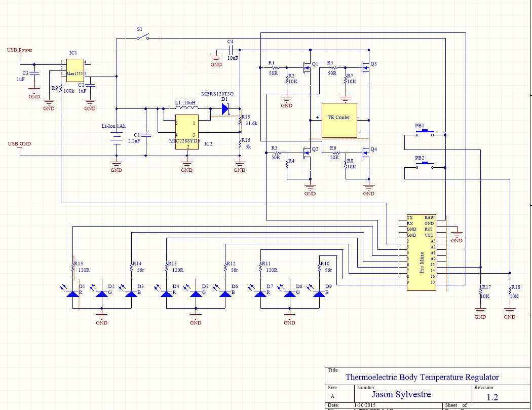
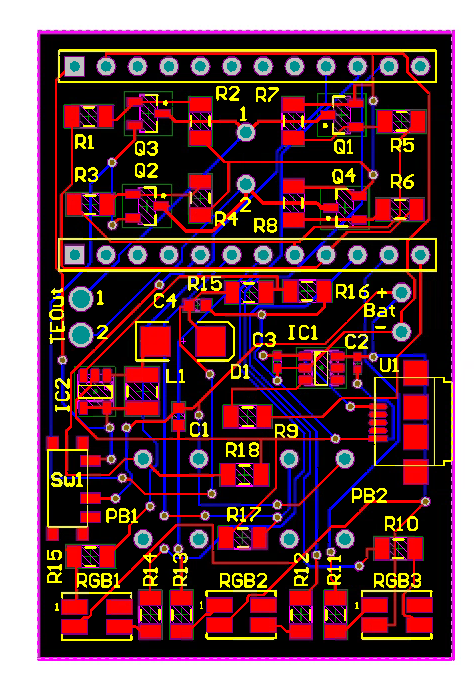
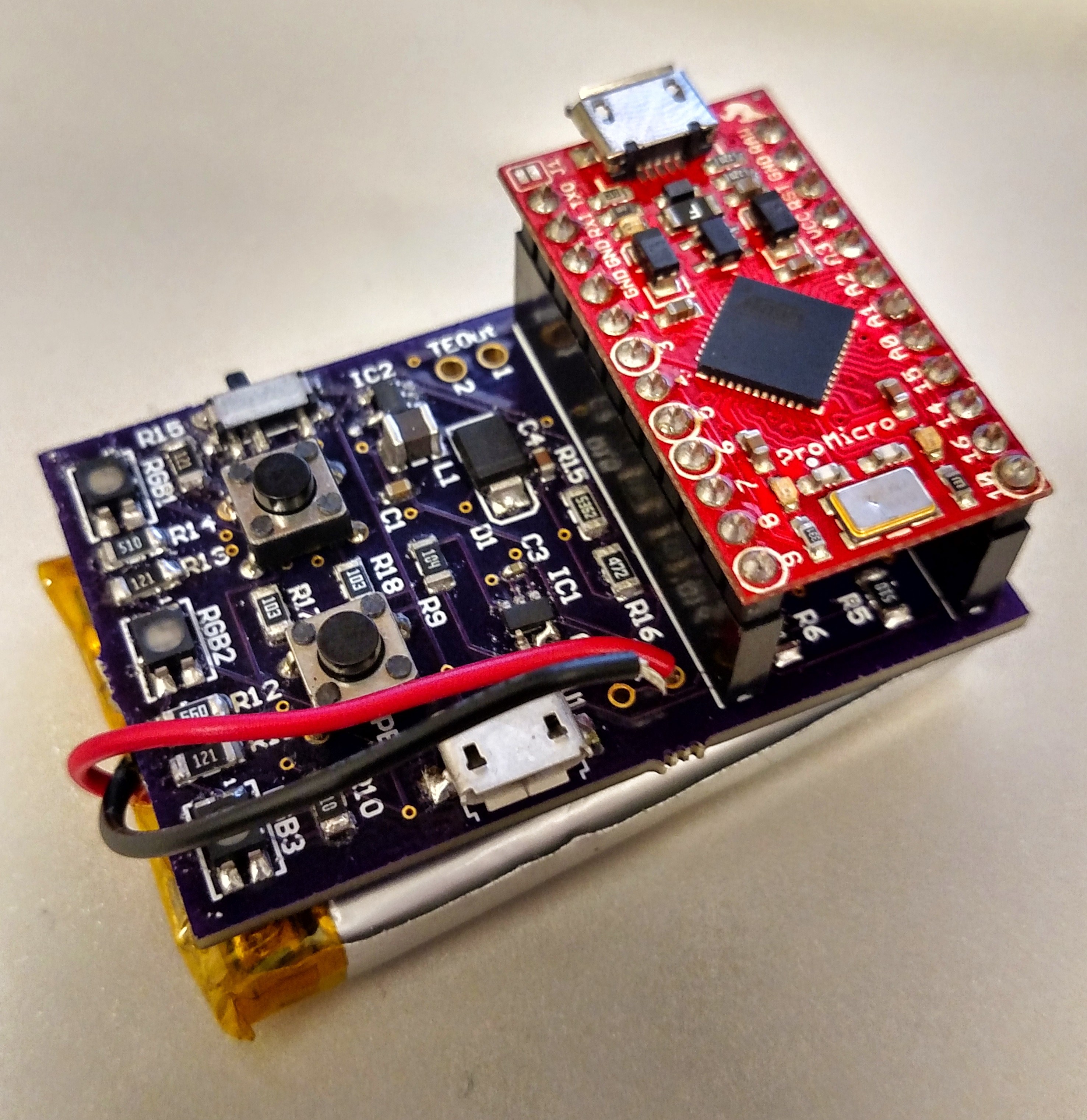
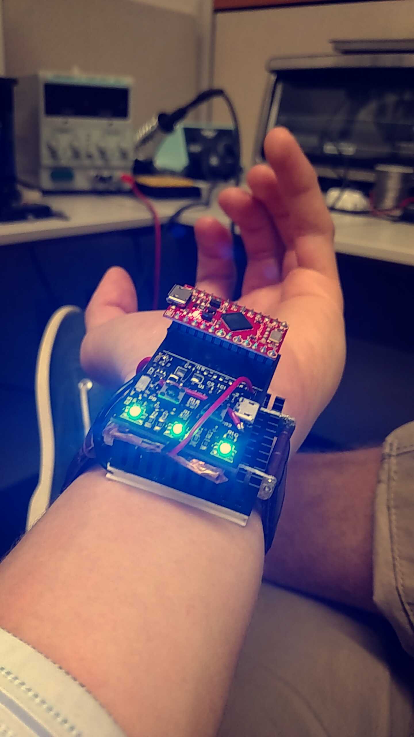
TEB is a thermoelectric bracelet that can be used for personal body temperature regulation. The current prototype uses a thermoelectric module in combination with a microprocessor to send automated pulsated thermal stimuli through the wrist to induce a perceptual change in body temperature. The effect is similar to putting your wrist in cold water on a hot summer day. This semester, I completed prototype 1.2, which was mainly composed of fixing issues that plagued with the first iteration prototype.  I had to redesign the circuitry and then also rewrite many aspects of my code to accommodate those changes.  I spent the majority of the semester testing and troubleshooting circuitry issues, but after many hours in the lab, I was able to get it working to a point where you can actually feel the pulses of cool stimuli running through your wrist.


2) Describe your overall feelings about the project. Are you happy, content, frustrated, etc with the results?

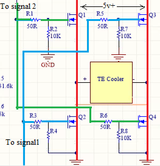
As with any engineering project, there are times of frustration and times of great satisfaction. With this project, it was particularly frustrating to see that the root cause of all my problems stemmed from my lack of understanding in the difference between P-channel and N-channel MOSFETs.  This problem really slowed me down and as a result, I did not get as much done as I would’ve liked this semester. However, I did learn a lot about circuit testing and analysis methods because of this and I am glad that I figured out what the problem was

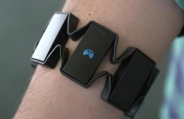
In terms of how well the device worked, I am very happy with its performance. The pulse frequency on the current prototype has by-no-means been optimized, yet it still cooled me down and made me comfortable during the symposium that I presented at. I was impressed with how quickly the the thermoelectric module can heat up and cool down.  Still though, the prototype is too bulky and not impractical and requires size reduction in order for this to be feasible.


3) What were some of the largest hurdles you encountered over the semester and how did you approach these challenges.

As stated earlier, the most difficult part this semester was identifying the circuit design flaw that was causing the circuit to short. To solve this issue, I used a systematic approach and tested each subsystem (i.e. voltage boosting section, H-Bridge section, USB charging section, LED section, and Processor section) using various methods and eventually identified that the H-Bridge configuration was causing issues. From there, I analyzed each component in the system to ensure it was soldered properly and that there were no bridges. I didn’t make much headway with that method so I removed individual components and tested it until it worked. Eventually, I found that when I removed one P-ch and one N-ch MOSFET from the board, the circuit worked. From this, I was able to determine my error in design.


4) If you had more time, what would you do next on your project?

 Revisions for Next Iteration

  • Minimize size to make it less cumbersome
  • Add heatsink to side that is contact with wrist
  • Use FET array chip instead of current configuration
  • Discrete processor chip instead of an off-the-shelf board
  • Remove voltage boosting circuitry
  • Use elastic band instead of watch band
  • Integrate circuitry into the band

Future Work

  • Redesign current board based on revisions stated above
  • Optimize pulse frequency to maximize the brain’s perception of your body changing temperature
  • Perform user study to see if it improves subjects’ thermal  comfort in warm or cool environments
  • Publish results


5/6/2015 TEB Update

These last two weeks, I have been bogged down by finals which hasn’t left me much time to work on the new for the next iteration of the TEB. However, I was able to finish the electrical schematic for Rev 2.1, which you can see below. The circuit will be much simpler than the previous iteration as I was able to eliminate many components with this new design. Below are the changes.

  1. No need to boost the voltage so I got rid of the voltage regulator chip and the accompanying circuitry
  2. Transistor configuration into a single FET array chip -http://www.diodes.com/datasheets/DMHC3025LSD.pdf
  3. Smaller Lithium battery will be used, haven’t decided on the form, but am looking at lithium coin cells
  4. Different battery charging management IC  http://ww1.microchip.com/downloads/en/DeviceDoc/22036b.pdf
  5. Atmel chip microprocessor will be used instead of the whole Sparkfun Pro Micro (have not implemented in schematic yet)
  6. Battery monitor IC to indicate when battery is low

Note: This is only the first draft. I still need to run a design analysis and check for errors.

T


4/19/2015 TEB Update

Last week, I presented my project at the Undergraduate Research Symposium marking the culmination of my work to this date. Unfortunately, it didn’t quite reach my expectations as I had very little traffic in regards to actually presenting my research to someone who is not familiar with it, which is too bad because the two people I did present to were very impressed with how it turned out.

I was able to get a functional prototyping working last week, which was very exciting. You can actually feel your wrist picking up the pulses of thermal stimuli from the cooler and it tricks you into thinking your body is cooler!  I was using during the Symposium because it was quite warm in that room and I was able to use TEB to achieve thermal comfort. I must say that I was surprised with how well it worked.

Undergrad Research symposium jpg

Now, onto the future of this project. The next step in this project will be to do a complete redesign of both the circuit and the physical bracelet. As I stated in the previous post, in this next iteration of the electrical design, I will remove the transistor configuration and replace it with a H-Bridge IC and I can remove the voltage boosting section of the circuitry. This will drastically reduce the size. Then I plan to change the wrist strap to make it less cumbersome to put on. The goal would be to have it closely resemble a Myo armband in terms of esthetics and size like the one in the image below.

http://cdn.techfrag.com/wp-content/uploads/2014/07/myo-armband-620x400.jpg

http://cdn.techfrag.com/wp-content/uploads/2014/07/myo-armband-620×400.jpg

4/10/2015 TEB Update

There is quite a lot of progress that has happened since my last post, but I’m going to start with the most significant breakthrough I had.  I found the source of all my problems and it stemmed from my lack of understanding of the difference between N-channel and P-channel MOSFETs. I understood that P-channel MOSFETs were used to switch HIGH side voltages, but I did not understand that the logic was the inverse to N-ch MOSFETs! What this means is that I did not know that in order to close P-ch MOSFETs, you need to pull the Gate voltage LOW. I’ve used N-ch MOSFETs in my day so, intuitively, I  thought P-ch was turned on the same way as N-ch; pull the Gate HIGH.  Boy, was I wrong. So now onto what this means for my application. I have the gates of my N-ch and P-ch MOSFETs connected (HeatPulse and ColdPulse) so when HeatPulse is set to HIGH, there is a direct short to GND because the other P-ch remains closed since the gate is being pulled LOW by a pulldown resistor. This is shown below

H-Bridge issues

There are a few solutions to this. One would be to implement an inverter between the MCU and the P-ch MOSFETs to invert the signal. The better solution I see though to purchase an H-bridge IC. This would eliminate many problems.

I also tested the thermoelectric module at different Power values to see how pronounced the temperature differential was. It turns ou that @3.8v and 800ma, the temp gradient is more than substantial for this application. This means I can remove the voltage boosting circuitry for the next iteration of the PCB. Currently, I have bridged the batttery voltage directly to the source of the transistors.

And then also for the next iteration, I’m looking to change the form factor of the PCB so that it is integrated into the wrist strap. Right now, it’s too bulky and cumbersome so I plan make it thinner as well.


Next Week’s Work

For the symposium, I plan to just present the cooling feature with the voltage supplied either from a transformer connected to a wall outlet or the Lithium Ion battery. I need to remove the P-channel transistor and connected the voltage input of the thermoelectric module directly to Vsource. I need to consolidate the PCB, TE Module, heatsink, wrist strap, and battery into a single unit. Then I’ll play around with timing to get the optimal frequency of sending pulses.

3/24/2014 TEB Update

What I accomplished this week

The two main things I did this week was troubleshoot my circuit and I wrote up details of the test procedure that will occur.

So, last week, I ran into an issue where the MCU would shut off when I added the DigitalWrite(HeatPulse, HIGH); or DigitalWrite(ColdPulse, HIGH); to my code. This sends a HIGH signal to the gate of the transistors that allow current to flow to the thermoelectric module.  For ‘HeatPulse’ the high voltage bus connects to the positive lead and then the low voltage bus is connected to ground.  When this occurs, heat is drawn from one side of the TE module to the other.  For ‘ColdPulse’, the polarity is reversed and causes heat to be transferred in the opposite direction. This system of transistors to enables a voltage to be applied across a load in either direction is called a H-Bridge.

As stated earlier, when I send a signal to trigger these MOSFETs, it shuts down the MCU. I measured the initial battery voltage and it was 3.7v and when the signal was sent, it was only 0.8v. So based on those observations, I reasoned that the large current draw from the thermoelectric module is causing the voltage to dip so I need to try a stronger power supply. Ross was kind enough to provide me with a computer power supply that had 3.3v, 5v, 9v, and 12v in abundance quantities, unlike my little battery. So I found the 3.3v line in the jumble of cables and desoldered my battery and soldered the power supply lines to my board. Unfortunately, the test results were less than desirable. The circuit board booted up and in less than five seconds, I noticed smoke coming from my board. It took me a bit to identify which component was burning up, but then I noticed the position of the inductor had shifted. Yes, the pads had heated up past the melting temperature of the solder. I fried the inductor in the voltage boosting sub-circuit.Inference: There is a short that appears only when either set of transistors’ paths

Unfortunately, the test results were less than desirable. The circuit board booted up and in less than five seconds, I noticed smoke coming from my board. It took me a bit to identify which component was burning up, but then I noticed the position of the inductor had shifted. Yes, the pads had heated up past the melting temperature of the solder. I fried the inductor in the voltage boosting sub-circuit.Inference: There is a short that appears only when either set of transistors’ paths

Inference: There is a short that appears only when either set of transistors’ paths are closed. This could be a design issue or fabrication issue (i.e. soldered incorrect component or accidental solder bridge, wouldn’t be the first time)

After hours of testing the circuit and analyzing schematics and analyzing PCB layouts, I have yet to determine the exact cause of the circuit though.

Next Week’s Work

I am going to discuss via email with Kevin Ponto who is currently in France for a VR conference and hopefully, we can diagnose the issue. If we cannot, then I am going to make a sacrifice and go with only cooling so I’ll have something presentable for the Undergraduate Research Symposium.

3/17/2015 TEB Update

What I accomplished this week

I spent this week testing and debugging my code. Unfortunately, I didn’t get as much as done as I would’ve liked to due to midterms.  I was able to manage to integrate the external interrupts into my code so now when I press  Pb+, it adds 1 to the counter and when I press Pb-, it subtracts 1. The processor determines the pulse frequency of the thermoelectric module depending on the value of the counter.  An issue I ran into was that the buttons were too responsive so when I pressed the pushbutton once, the processor registered it as me pressing it several times. To solve this, I need to add millis() to my code to delay it.

Next week’s work

It’s going to be a very busy three weeks leading up to the Undergraduate Research Symposium on April 16. Once I finish coding this I still need to perform a user study to get some test data from several human subjects in a controlled environment.  Next week, I would like to get my code working and write up a description of the details of the tests.

3/9/2015 TEB Update

What I accomplished this week

This week, I wrote the new code with the external interrupts implemented. If you read my post last week, you’ll know in the previous iteration, there was a large delay in program response when the buttons were pressed. The push buttons are now connected to the external interrupts on the AVR so this hardware solution should help eliminate the delay issues. For those of you who don’t know, external interrupts are a feature processors have to eliminate the slow timing of the polling process of I/O devices. The protocol usually is something like this

  1. The processor notices a state change on the interrupt pin.
  2. The main loop stops what its doing and saves its current state
  3. The Interrupt Service Routine (special kind of function) executes its code
  4. Data from the the ISR is transferred to the main loop using global variable
  5. Main loop starts where it left off with the data change

Of course, it is much more complicated than that on a hardware level, but that is the general idea

So I have my program set up where the push buttons are connected to the two external interrupts and then a push button counter that keeps track of which of the two push buttons have been pressed and how many time. The range is (-3, 3) with -3 being the coolest level and 3 being the warmest level so there are 3 cooling levels, 3 heating levels, and 0 is neutral (off).  I have two different ISRs, one to increase the value of the counter and the other to decrease it. And then there is the main loop, which sets the pulse frequency and LED level depending on the value of the counter.

I compiled the code and received no syntax errors.

Next week’s work

I would like to test the code on the board and fix any bugs with it. I am also going to meet with Professor Kevin Ponto to see if my code is as efficient and concise as it can possibly be.


3/2/2015 TEB Update

What I accomplished this week

All my time this week was spent solving the electrical issue that was causing a short circuit (actually very high resistance, but not infinite) which prevented the circuit from functioning properly.  After spending a few hours with Professor Kevin Ponto analyzing and testing different subsystems of the circuit, we identified that the issue was coming from the H-Bridge section of the circuitry. I checked my design twice and verified that there weren’t any problems with it. This meant that there was an error when populating the board.

What I found was that I mixed up the location of two transistors when populating the board. There was a P-channel where an N-channel was supposed to be and vice verse.   I then removed and swapped the transistors and sure enough, everything is working perfectly now.

See the image below for more details.

Next week’s work

I would like to finish writing and testing the code out on my board.  The reason I have to write new code for this iteration is because I modified the PCB design so that the buttons are now connected to the external interrupts on the microcontroller.  This should help eliminate the delay issues (when the buttons were pressed) I was having with my first iteration.

1_30_2015 PCB2 Analysis (3)

The transistors in the white boxes were the root of my issues. I had one N-channel and one P-channel in each box, this enabled current to flow directly from power to ground. Q2 and Q3 in the left box should be two P-channel transistors and Q1 and Q4 in the right box should be two N-channel transistors

2/23/2015 TEB Update

What I accomplished this week

This last week, I was trying to identify where the problem was in my design that was causing the results that were outlined in the previous post. I thought I identified the problematic trace which is the one connected to the white circled via in the bottom right corner in the image below.

1_30_2015 PCB2 Analysis (1)

This is the trace that connects the common anode of the LEDS to the source voltage. The idea is that when you want to turn on one of the LEDs, you pull that signal pin LOW instead of HIGH and that will give the polarity needed to turn on the LED.  However, as you can see from the image, this trace is not routed through the main power switch on the left (Sw1).  I deduced that this was the reason why the LEDS are turned on even when the power switch is off. To reroute this without having to fabricate another board, I cut the trace and then placed a jumper between the circled via and the output of Sw1

Test, Observations, and Problems

Before rerouting the trace, I uploaded some code the microcontroller that told the LEDS to turn blue on startup. With the switch off, I supplied a voltage and the red LEDs illuminated just as before. When I pressed the buttons, the microcontroller powered up and the blue LEDs turned on so that was successful. So I then rerouted the trace with hope that would solve the problem of the red LEDS illuminating when the switch is off and it did, but then that lead to another problem. When the switch was off, everything was off, but when you turned the switch on, the power LED on the microcontroller flashed for a fraction of a second and then shut off.

Next Week’s Work

Next week, I’m going to compare my old schematic to the new one and then remove components one by one to identify which section of the board is causing the issue. I also need to submit my application to present at the Undergraduate Research Symposium.

Also, a message to all readers, if you see the problem with my circuit, comment!

2/15/2015 TEB Update

What I accomplished this week

Testing, Observations, and Problems from Initial Bootup

This week, I powered up the board for the first time and I got mixed results. There was no magic smoke like last time and I didn’t fry any components, however, the MCU to go into shutdown mode.  There is something else very strange that is going on.  When the power switch is turned off, the LEDs are very weakly illuminated and the microcontroller power LED is off.  When the push buttons are pressed, the LEDs turn off and the power LED of the MCU turns on.

When the power switch is turned, there is no response from any of the components on the board.

Next Week’s Work

Next week, I’m going take another closer look at my schematics and PCB design to see if I can identify the problem. Once I identify the problem, I will make the necessary hardware changes to ensure proper function and will update my PCB and schematic accordingly.

Note: Below are images of the electrical schematic, PCB design, and the current prototype

1_30_2015 Schematic


1_30_2015 PCB2